Introduction
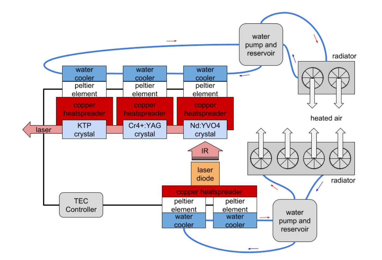
An important part of the Laser4DIY system is the cooling system. There are four components that need to be actively cooled: the laser diode, the KTP crystal, the Cr4+:YAG crystal and the Nd:YVO4 crystal. The laser diode is the component which the most demanding cooling requirements as it produces a lot of waste heat but at the same time needs to be held at a constant temperature to avoid fluctuations in wave length of the produced laser light.
Our approach is a low-cost cooling setup which combines the precision of thermoelectrical controlled cooling with the low cost of off-the-shelf CPU cooling components. As one can see in the figure below two cooling loops are used, one for the laser diode and one for the crystals.
Requirements and Similar Projects
The requirements for the temperature controller or more accurate TEC-Controller (TEC stands for thermo electric cooling and utilizes peltier elements to cool or heat without any moving parts) are coming from the project requirements themselves and the technical requirements for being able to cool the laser sufficiently. The general requirements are:everything has to be published as open source, every component has to be suitable to be soldered to the corresponding PCB by hand and finally it has to be as cost-saving as possible. The technical requirements are: being able to control four peltier elements simultaneously with 106W heat transfer capacity, which means to switch 12A at 15.5V. Furthermore it should be able to stabilize temperature of a laser diode within 0.3 K. A similar concept of a low-power open-source TEC-controller is already available at http://hololaser.kwaoo.me/electronics/Arduino_TEC/Arduino-TEC.html. The concept of the TEC-Controller developed for Laser4DIY is derived from this project, but heavily modified to meet the requirements. The core platform has been changed from Arduino Uno to Arduino Due. In course of that the voltage of the digital signals changed from 5V to 3.3V, which meant to change all other components to work with the lower voltage. The reason behind that is, that for four channels the Arduino Uno has not enough computing power to run the PID controller in software and not enough pins to run the switching hardware. Furthermore the power part of this particular TEC-Controller was designed to drive only small peltier elements with currents up to 3A, which is not enough for this project.
Principle of Temperature Control
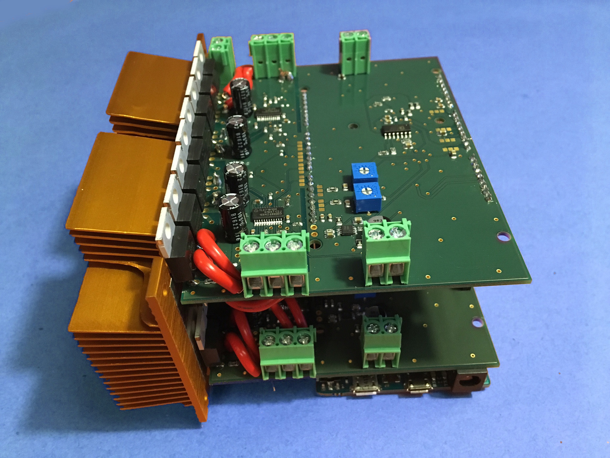
The principle of temperature control is very simple: There is an input screw terminal, to which a NTC (negative temperature coefficient) resistor, which is a component with temperature-dependent resistance, is connected. This NTC should be thermally coupled very strongly to the object whose temperature is intended to be be regulated. The temperature is read out over the microcontrollers ADC and compared in software with the setpoint. The software then steers the output controlled by a PID algorithm. The output is a PWM (pulse width modulated) signal, which means that it is a square wave with fixed frequency but varying duty cycle. This signal is used by a H-bridge controller to drive the gates of four MOSFETs in H-bridge configuration. The output of those is connected to a screw terminal where the peltier element can be connected to. This whole control circuit is twice on one board and with two boards stacked on each other the Arduino Due has four control channels in total. Both boards are identical in design and can be configured to act as board with channels 1 and 2 or as board with channels 3 and 4 via solderbridges.
Development
Component Selection
After looking into the concept behind the TEC-Controller lets now look on the components chosen for the design. In general components are used which have leads and are solderable by hand. As written before, the processing is done by an Arduino Due, an open-source microcontroller board, which hosts a Atmel SAM3X8E ARM Cortex-M3 MCU and is programmable via C++ over an integrated development environment (IDE). Also the 3.3V voltage supply sits on the Arduino board and the TEC-Controller utilizes the standardized socket on the Arduino to connect to it. To measure the temperature a voltage divider is used and its output is then amplified and stabilized by an op-amp, the OP484FSZ by Analog Devices. It was chosen because of its low temperature drift and the capability to run with 3.3V supply voltage. For the ADC in the MCU to be able to measure the voltage accurately a 3.3V voltage reference was used, the REF6133 by Texas Instruments. For driving the the MOSFET gates a TLE718EM by Infineon was used, which is a H-Bridge driver and can, thanks to its package, also be hand soldered. Finally for switching the peltier elements 8 MOSFETs (4 for each of the both channels) were used. The chosen IRLZ34NPBF is a N-Channel MOSFET capable of switching up to 27A at 55V. These MOSFETs are some of the few through-hole components and have been mounted altogether to a heat-sink via M3 machine screws. As the external power supply unit (PSU) a no-name 15V constant voltage power supply capable of delivering up to 50A was chosen.
Component Design
After choosing the components some of them need external configuration by passive components:
Op-Amp gain: Since the range for voltages coming out of the temperature measurement by the voltage divider is about 1.2V-1.6V in the temperature range of 15-24°C, an amplifier is needed to utilize the whole voltage range (0-3.3V) of the ADC. The configuration of the op-amp is done by external resistors. The non-inverting amplifier circuit with offset voltage is used to amplify the voltage and bring it to the right level (see also Equ. 4.3). The output is then about 0-3.3V for the already mentioned 15-24°C. The resistor values chosen are: R1, R5 = 23.7kOhm und R2, R3, R4 = 10kOhm. For the second channel the same values are used. A second configuration for the range of 5-55°C is: R1=R2=R4=10k, R5=2.7k, R3=not populated.
Short detection: The H-Bridge driver TLE7181EM offers an integrated op-amp for current sensing including over-current or short detection, whose gain has to be defined by a resistor network. The formulas for calculation of R31-R36 can be found in the TLE7181EM datasheet on page 23: The gain is RFB/RS, where RFB = 1/(1/RREF1 + 1/RREF2). To find the right gain the first thing is to look into the maximal voltage drop which can be induced by the shunt resistor for current measurement. This is because of the shunt resistance of 2mOhm is about 24mV at 12A current. Since the target voltage range for the built-in ADC of the Arduino is 0-3.3V a gain of 100 is chosen. This would convert the 0-12A to 0-2.4V. To reach this gain value first of all the RFB has to be chosen, 100kOhm is a good choice in such cases. The next value is then RS, which is RFB/GAIN or 100kOhm/100 = 1kOhm. Dropping this into the equation for RFB, one gets 200kOhm for RREF1 = RREF2. This also means that the over current threshold is at about 25A. To sum up: R31 = R32 = 1kOhm, R33 = R34 = 100kOhm and R35 = 200kOhm. For the second channel the same values are used.
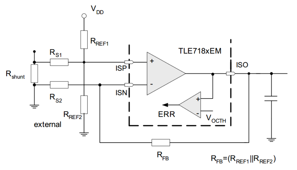
Schematic of H-Bridge current sensing. Taken from the TLE7181EM datasheet
- Deadtime (DT): To ensure that the MOSFETs which would otherwise connect the power supply to ground are not switched on at the same time, the H-bridge driver waits for a certain time in between switching these MOSFETs. This is called the deadtime and should be of the magnitude of the maximum switching times of the MOSFETs. These depend on the one hand on the switching times of the MOSFET core itself, on the other hand they are limited by the charge up time of the gate. This can be calculated by the current equals charge over time equation I=Q/t, where the following values are put into: The MOSFET gate charge Q = 25nC, the maximum can be expressed the maximum voltage at 11V and the gate resistor with 20Ohm, so the result is 50ns. To this value the internal propagation delay with 200ns has to be added, which results in 250ns. Including a safety factor of 5, 47kOhm as RDT was chosen, which results in 1200ns deadtime.
Schematic
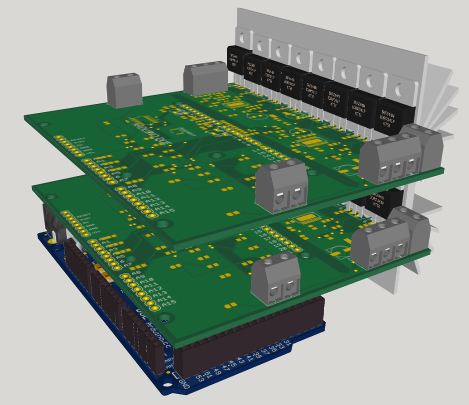
The schematic itself is separated into four parts: The first one is the socket for the Arduino Due, which is placed in the center and includes some filtering capacitors and the jumpers for configuring the PCB. The second part (the top one) is used for the temperature measurement, with the op-amp and the voltage reference. The third and fourth part are identical and consists of the H-bridge driver and the MOSFETs.
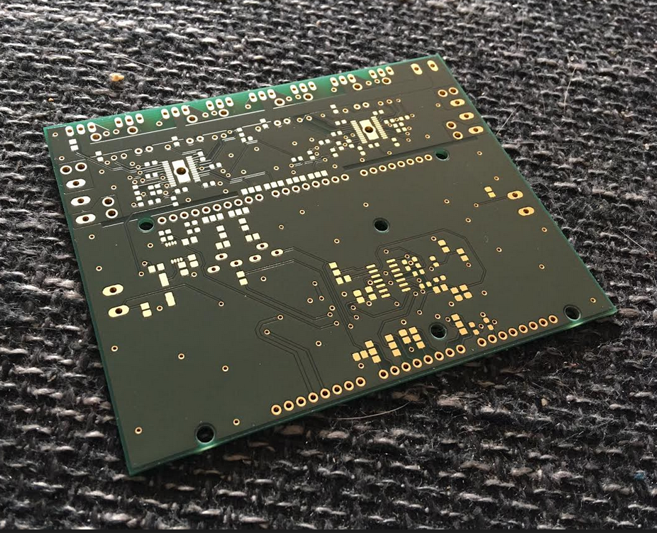
Layout
For layouting there is a limited board size, which is a restriction of the layout software. The board outline should not exceed 10,7 cm x 8,4 cm. To give hobbyist and fablabs the opportunity to recreate the PCBs by traditional methods, a two layer setup was chosen. Additionally, to be able to transfer high currents, as a copper layer thickness 70µm were chosen. With this thickness the width of the high power traces could be calculated [51]: they have to carry up to 12A and therefore should be at least 3.81mm wide. The layout (see Fig. A.2) is divided into two parts: the measurement and the power part. Both are separated through a gap in the copper planes to prevent the measurement part to be heated up by the power part. Furthermore, to prevent electronic noise in the measurement part, the ground return line for the MOSFETs is also separated and only connected through a small bridge to the rest of the board. The spacing between the parts has been kept big enough so every component can be soldered by hand. By the same reason a big via has been placed under the H-bridge driver to be able to solder the ground pad on the underside of the part from the other side of the board. Finally to be able to connect the MOSFETs gates over the power lines, through hole resistors have been introduced to bridge the gap (also see upper part of Fig. A.2).
Software
The software is based on an already existing project and modified to run with the the hardware developed in this thesis. Besides smaller modifications the in- and output pins has been changed to the actual ones, the one channel sensing and control was extended to be able to work with four channels and the over-current functionality was removed since its implemented in the H-bridge driver. In the software runs a main loop, where the ADCs are read out, the PID algorithm is called to calculate the output and this output is then sent out to the H-Bridge drivers. Before the main loop is executed, the setup routine is called, where the serial communication, the in- and output pins and the PID controllers are configured.
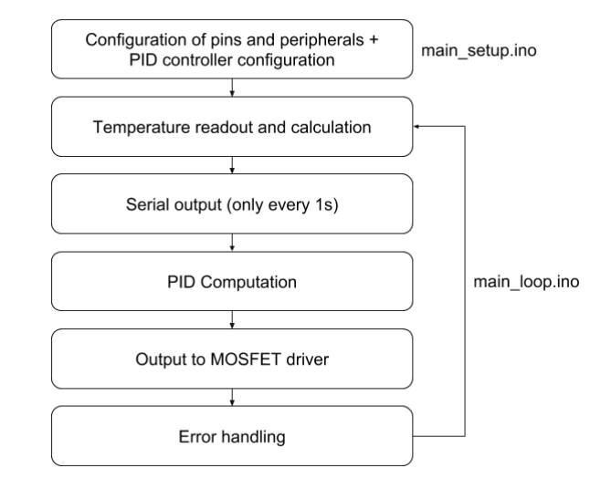
Schematic of the software of the TEC-Controller