[English version] [zur deutschen Version]
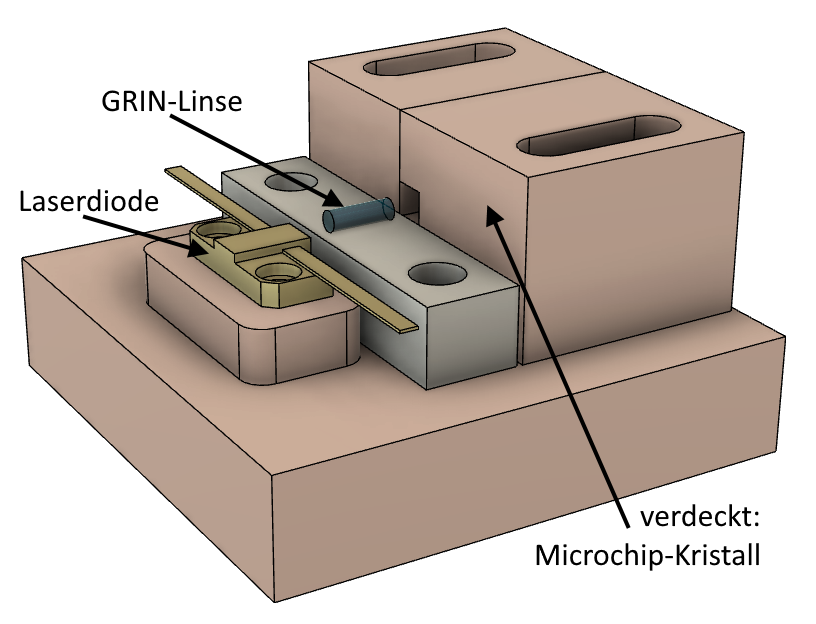
Laser4DIY uses a laser with a microchip resonator as the basis. A free-beam diode generates pump radiation with a wavelength of 808 nm, a symmetrical beam divergence of 8°×8° and an emitter size of 200 µm. A GRIN lens (GRAdient-INdex lens) with a focal length of 1.95 mm and an anti-reflective coating for 830 nm on both sides focuses it on a narrow area in the microchip crystal, which increases efficiency.
A special heat sink was designed for a compact structure, which holds and cools the laser diode, the GRIN lens and the microchip crystal:

The Microchip crystal consists of a Cr:YAG based passive Q-switch, a Nd:YAG crystal and an undoped YAG crystal fused together. The undoped YAG crystal is used here for more efficient heat dissipation and a reduced thermal lens as a result. The resonator mirrors and anti-reflection coatings for the pump radiation are vapour-deposited on the end faces. In the course of the tests, several combinations for the individual areas of the diffusion-bonded crystal were tested.
The HR coatings were occasionally damaged by the high peak powers in the microchip resonators. Unfortunately, simulations could not provide usable results here, which is why crystal parameters were adjusted iteratively. The best and most robust properties were realized with the following crystal:

The crystal has the dimensions 3 × 3 × 9 mm³ and is doped with 1% Nd. The output surface has a reflectivity of 60% at 1064 nm and the input surface has a reflectivity of >99.5% at 1064 nm and <0.5% at 808 nm.
A pump diode with a maximum power of 10W and an emitter size of 200 μm with a beam divergence of 8° × 8° is used in the laser setup. With a pump power of 8.9 W (10A at 1.9V), this setup achieves an average output power of 1.36 W at 1064 nm. The pulse length is around 2.5 ns (FWHM) at a repetition rate of 11.3 kHz. A pulse energy of 120 µJ and a peak power of almost 50 kW can be calculated from this. The temperature is set in such a way that the maximum emission of the microchip crystal occurs at 1064 nm, in our case it was 16.1 °C.
The construction of the laser source is possible in two variants, one with an optical amplifier and one without it. While an amplifier with the use of additional components and the associated additional costs naturally results in a higher output power, the result without amplification is a more cost-effective, less complex system.
The microchip laser just described serves as the basis. The divergent laser beam from the microchip crystal with λ= 1064 nm is expanded and collimated using a double beam expander (L1 and L2 in the figure below).
The amplifier module can be integrated after the first deflection mirror M1. It is mechanically similar to the Microchip module, but has a dichroic mirror (MV) below 45°, which has an AR@1064nm coating on both sides and an HR@808nm coating on the side facing the amplifier crystal. This can be pumped via the lens LV with 808 nm or 878 nm via a fiber-coupled pump diode.
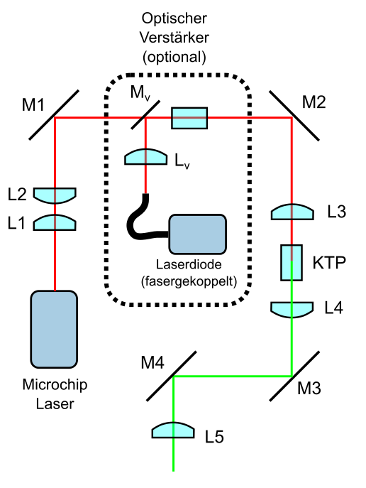
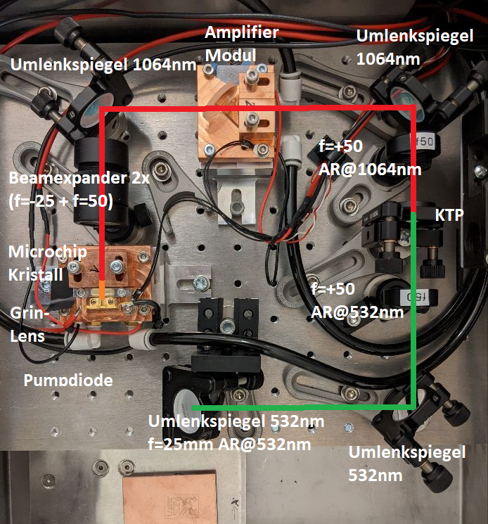
Schematic structure of the laser (left) and structure in the device (right, with amplifier module but without the pump diode)
After the second deflection (M2), the 1064 nm beam is focused into the KTP crystal by an f=+50mm lens. The KTP crystal is adjusted in rotation around the beam axis and angle to the beam axis for maximum conversion efficiency.
After frequency doubling, another f=+50mm lens collimates the resulting laser beam at 532 nm. The following two mirrors (M3, M4) direct the beam down through an opening in the optical plate where the traversing unit is located. M3 and M4 only have an HR@532nm coating and transmit only approx. 50% of the power at 1064 nm, which is therefore not relevant for the later ablation process.
A lens with f=25mm (L5) sits in the opening of the breadboard, which focuses the laser beam onto the board to be processed.
The temperatures of the pump diodes are adjusted to maximum power output to ensure the best possible absorption. During the first adjustment, the KTP crystal should be moved step by step from a distance at least 1 cm greater than the focal length of the lens to the focus in order to avoid laser-induced damage to the crystal.
With the output of the microchip laser described above (1.36 W average power), an average power of 0.25 W at λ= 532 nm could be achieved with this setup. This corresponds approximately to a pulse energy of 20 µJ and a peak power of approx. 9 kW. With an assumed focus size of 40 µm, this results in a peak power of over 1200 MW/cm² on the surface of the circuit board.
With this setup, standard copper coatings on a circuit board (35 µm thick) could be removed completely and electrically isolating with a travel speed of 40 mm/min and two passes. The ablation takes place over a width of approx. 15-20 µm, which enables very fine details.
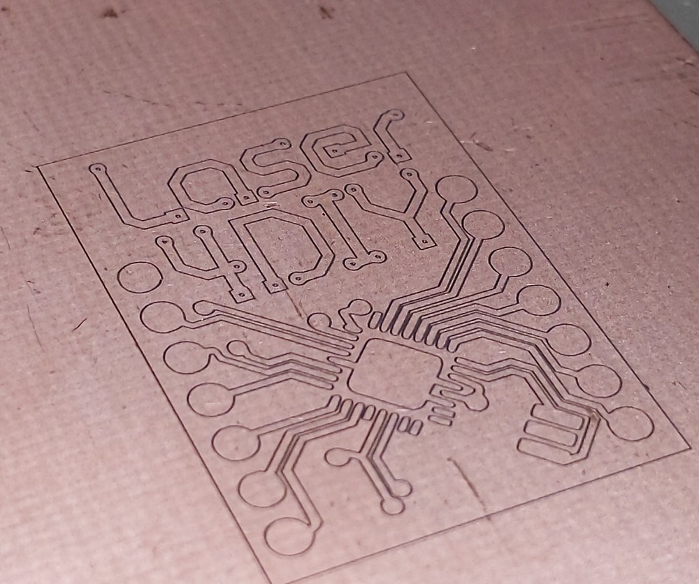
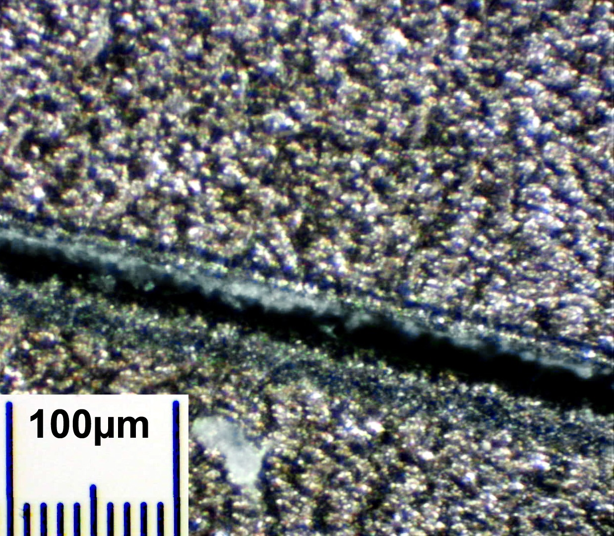
Circuit board created with the Laser4DIY device (left), microscope view of an ablation (right)
The functionality of the setup with optical amplifier was successfully verified . A pump diode was used for this purpose, which was provided free of charge by Wematec GmbH. Research into possible suppliers for a pump diode that could be considered for use in the Laser4DIY system in terms of cost and integration of the optical amplifier into the documentation was initially refrained from and is reserved for possible future research work.
The cooling of the components - in the case of the structure with bounce geometry in particular the 60W pump diode - proved to be problematic right from the start of the project and various configurations were tested. The system has been optimized over several iterations so that it is now suitable for the designed laser setups.
Basically, peltier elements are used to cool or stabilize the temperature of the critical components. The waste heat generated is dissipated by water cooling using radiators. The figure below shows a schematic overview of the cooling system:

Schematic structure of the cooling system (variant structure with bounce geometry)
While relatively inexpensive standard components from PC technology are used for the water cooling, including the pump, expansion tank and radiator, tailor-made copper heat sinks are required for the laser diode, the laser crystal and the microchip laser:
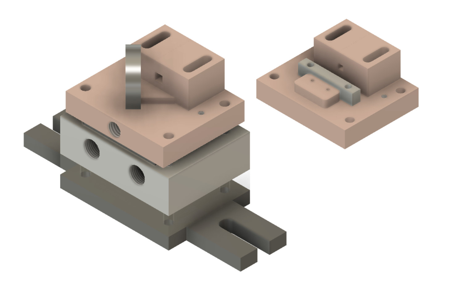
On the left you can see the overall structure for the amplifier module, in which highly integrated copper heat conductors with functional surfaces for gluing optical components, peltier element, heat sink, acrylic sealing plate and base plate with fastening lugs for an optical table are screwed together to form one component. The structure for the microchip laser is identical in construction, but only differs in the upper part made of copper. This upper part with various functional surfaces for installing the laser diode, GRIN lens and microchip crystal can be seen on the right.
Parts of the cooling system of the Laser4DIY device, namely radiators, water pump and expansion tank are in a separate supply unit:
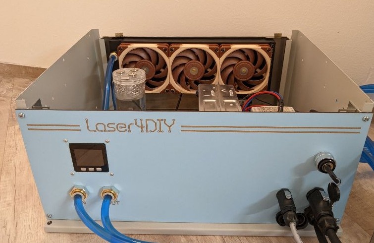
Opened supply unit: on the left the expansion tank with integrated pump, at the back the radiators of the cooling system