...
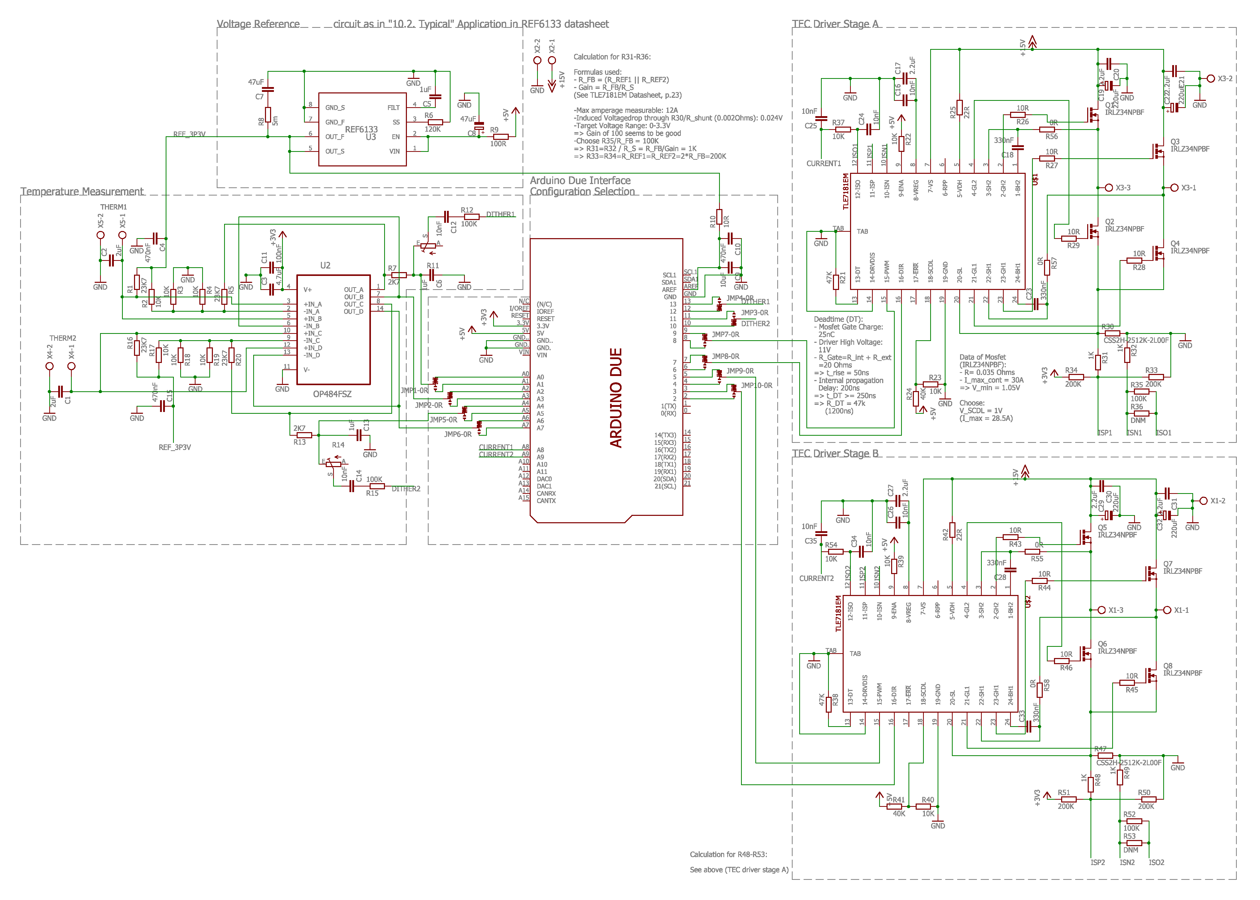
The schematic itself is separated into four parts: The first one is the socket for the Arduino Due, which is placed in the center and includes some filtering capacitors and the jumpers for configuring the PCB. The second part (the top one) is used for the temperature measurement, with the op-amp and the voltage reference. The third and fourth part are identical and consists of the H-bridge driver and the MOSFETs.
Layout
For layouting there is a limited board size, which is a restriction of the layout software. The board outline should not exceed 10,7 cm x 8,4 cm. To give hobbyist and fablabs the opportunity to recreate the PCBs by traditional methods, a two layer setup was chosen. Additionally, to be able to transfer high currents, as a copper layer thickness 70µm were chosen. With this thickness the width of the high power traces could be calculated: they have to carry up to 12A and therefore should be at least 3.81mm wide. The layout is divided into two parts: the measurement and the power part. Both are separated through a gap in the copper planes to prevent the measurement part to be heated up by the power part. Furthermore, to prevent electronic noise in the measurement part, the ground return line for the MOSFETs is also separated and only connected through a small bridge to the rest of the board. The spacing between the parts has been kept big enough so every component can be soldered by hand. By the same reason a big via has been placed under the H-bridge driver to be able to solder the ground pad on the underside of the part from the other side of the board. Finally to be able to connect the MOSFETs gates over the power lines, through hole resistors have been introduced to bridge the gap.
...