Introduction
An important part of the Laser4DIY system is the cooling system. There are four components that need to be actively cooled: the laser diode, the KTP crystal, the Cr4+:YAG crystal and the Nd:YVO4 crystal. The laser diode is the component which the most demanding cooling requirements as it produces a lot of waste heat but at the same time needs to be held at a constant temperature to avoid fluctuations in wave length of the produced laser light.
...
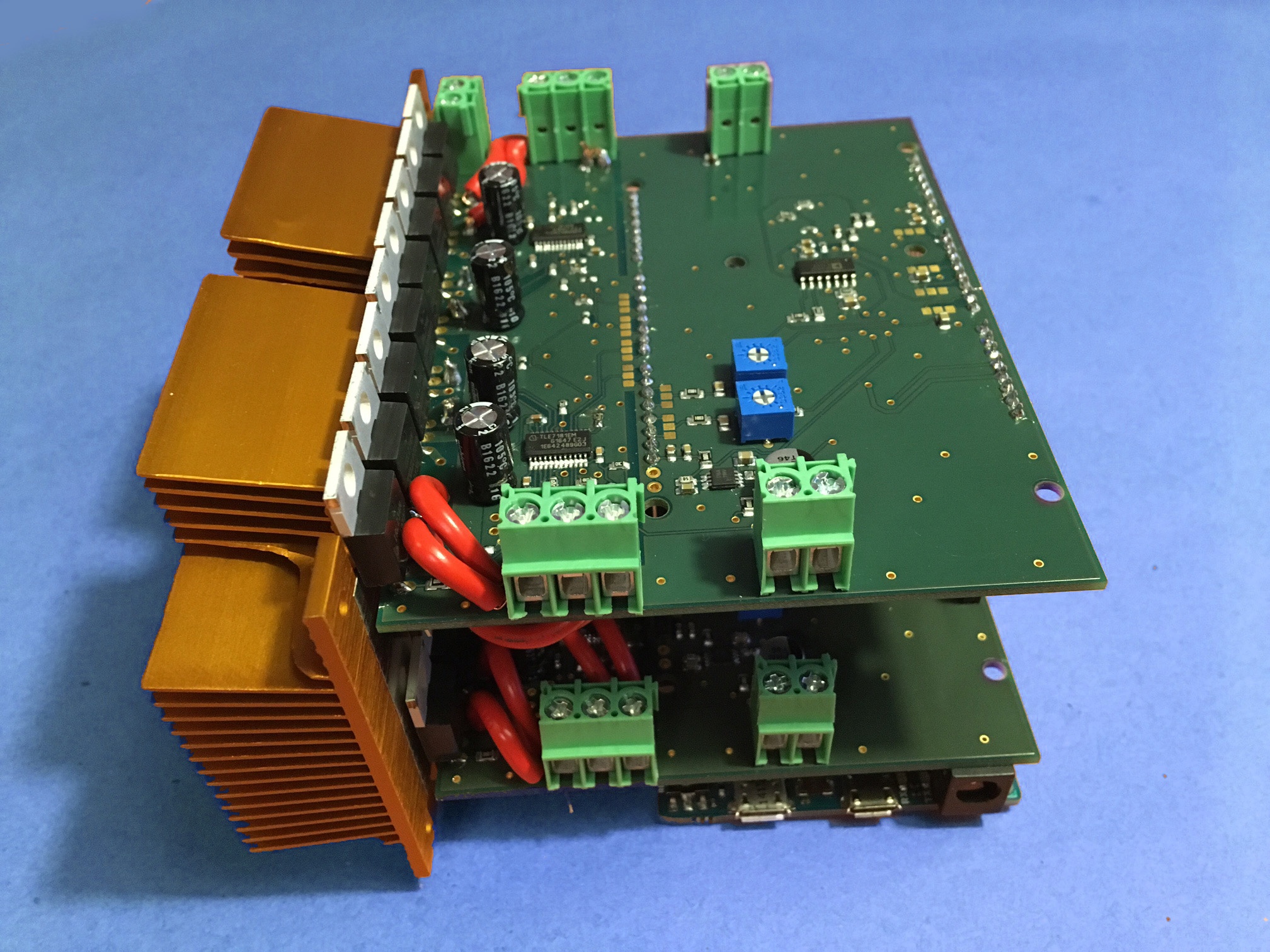
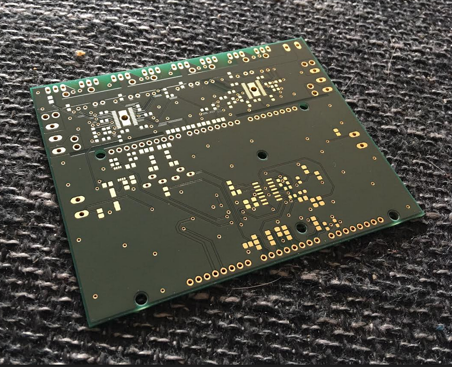
For layouting there is a limited board size, which is a restriction of the layout software. The board outline should not exceed 10,7 cm x 8,4 cm. To give hobbyist and fablabs the opportunity to recreate the PCBs by traditional methods, a two layer setup was chosen. Additionally, to be able to transfer high currents, as a copper layer thickness 70µm were chosen. With this thickness the width of the high power traces could be calculated [51]: they have to carry up to 12A and therefore should be at least 3.81mm wide. The layout (see Fig. A.2) is divided into two parts: the measurement and the power part. Both are separated through a gap in the copper planes to prevent the measurement part to be heated up by the power part. Furthermore, to prevent electronic noise in the measurement part, the ground return line for the MOSFETs is also separated and only connected through a small bridge to the rest of the board. The spacing between the parts has been kept big enough so every component can be soldered by hand. By the same reason a big via has been placed under the H-bridge driver to be able to solder the ground pad on the underside of the part from the other side of the board. Finally to be able to connect the MOSFETs gates over the power lines, through hole resistors have been introduced to bridge the gap (also see upper part of Fig. A.2).
Software
The software is based on an already existing project and modified to run with the the hardware developed in this thesis. Besides smaller modifications the in- and output pins has been changed to the actual ones, the one channel sensing and control was extended to be able to work with four channels and the over-current functionality was removed since its implemented in the H-bridge driver. In the software runs a main loop, where the ADCs are read out, the PID algorithm is called to calculate the output and this output is then sent out to the H-Bridge drivers. Before the main loop is executed, the setup routine is called, where the serial communication, the in- and output pins and the PID controllers are configured.
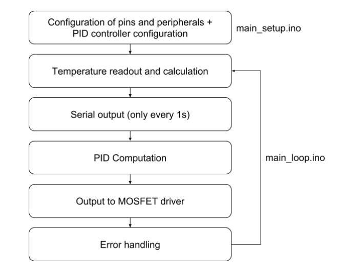
Schematic of the software of the TEC-Controller